The clean your yield depends on.
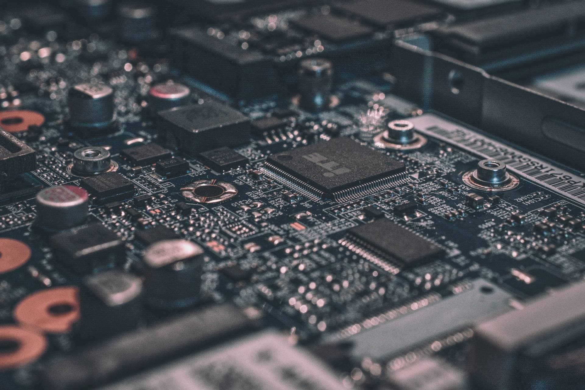
At 3 nm and below — where a single node is barely 20 atoms thick — atomic-level contamination limits yield, reliability and power. SisuSemi's ALP™ cleans silicon surfaces at the atomic layer, so the next generation of chips can keep scaling.
Illustrative image. Published results vary by device class — see case studies for specific numbers.


At today's nodes, particle cleaning isn't enough. Atomic-level impurities dominate what devices do.
Traditional cleans stop at particles.
Conventional wet and cryo cleans remove particulates but leave sub-nanometre contaminants (hydrogen, carbon), disordered chemically-grown oxide, and atomic-scale interfacial defects behind. Those invisible residues drive leakage, variation and reliability loss at advanced nodes.
ALP™ operates at the atomic layer.
ALP™ removes hydrogen and carbon contaminants in UHV, reorders the disordered silicon surface, and grows a thin crystalline SiO₂ layer — verified by TEM — giving the device stack a clean, repeatable interface to build on.
UHV, laser heating, and controlled oxygen — not another wet clean.
The AtomSeal™ system combines Ultra-High Vacuum, uniform laser-based wafer heating (up to Ø300 mm), and controlled oxidation to strip atomic-level contaminants and regrow a clean, crystalline silicon-oxide interface.
- 01

Ultra-high vacuum
ALP™ runs in UHV — a regime silicon foundries traditionally haven't used. That's what makes true atom-level cleanliness reachable without re-contaminating during processing.
UHV chamber · AtomSeal™ system - 02

Uniform laser heating
Wafers up to Ø300 mm are heated uniformly with an IPG Photonics fibre-laser source — below 450 °C. Resistive heating can't match that uniformity or throughput scaling.
<450 °C · Ø300/200/150 mm - 03

Controlled oxidation
A precisely controlled oxygen flow regrows a thin crystalline SiO₂ layer on the ordered silicon surface — sealing and protecting it for downstream processing.
Thin crystalline SiO₂ (~1 nm, TEM-verified) - 04

Clean surface, ready for the stack
Hydrogen and carbon contaminants are gone, the surface is ordered, and the interface behaves the way your device design assumes it will.
Front- or back-end-of-line · FEOL/BEOL
The physics of clean, translated into fab KPIs.
Four headline outcomes customers have seen on their own silicon after ALP™ — measured on their own devices, against their own baselines.
At the Si surface and interface, atomic-level contaminants and disorder are removed — reducing defect density by 300–400% (3–4×).
Case studies show leakage reductions of 50% (photodetectors), 67% (MOSCaps), 75% (p-n diodes) and up to 80% (sensor sidewalls).
Lower leakage translates into chip-level power savings — a 50% boost in battery life for mobile-class devices.
Up to a 20% increase in usable chips per wafer, driven by a lower defect floor and tighter device-to-device variation.
Built for every step of the silicon value chain.
Differentiate chips and lift yield without rewriting your flow.
IDMs manage design and manufacturing. ALP™ helps you tighten defect density, lift reliability, and get more usable chips per wafer.
- Up to +20% manufacturing yield
- Lower defect rates, higher performance, longer lifespan
- Enables volume production of higher-density designs
A measurable edge in a crowded deal market.
Foundries compete against peers and IDM-owned fabs. ALP™ helps you offer lower defect floors, more consistent yield across batches, and stronger reliability.
- Significant reduction in defect density and leakage current
- Up to +20% yield — more usable chips per wafer
- Consistent quality across diverse client specs
Push design limits. Get to market faster.
Fabless teams rely on foundries to hit performance. ALP™ helps your designs hit spec and move through validation with fewer iterations.
- Faster time-to-market with fewer defects
- Consistent chip performance from foundry partners
- Atomic-level cleanliness raises the ceiling on design choices
Where atomic precision already pays for itself.
Dit reduced 42% and leakage cut 67% on Metal-Oxide-Semi capacitors.
Applied to MOSCap structures used in memory, logic and sensor chips. SisuSemi's surface treatment reduced interface defect density (Dit) by 42% and leakage current by 67%, while STEM imaging confirmed the amorphous silicon oxide had re-ordered into a crystalline Si/Al₂O₃ interface.

Photo-detector leakage reduced by 50% for better sensitivity.
A leading photodetector manufacturer had leakage current limiting sensitivity and signal accuracy. ALP™ treatment applied to diced components reduced leakage by 50%, improving detection accuracy and light sensitivity without compromising other characteristics.
Leakage cut 75% on particle detectors with improved radiation hardness.
Particle detectors for satellites and nuclear power plants faced excessive p-n diode leakage in harsh radiation environments. ALP™ treatment on diced components reduced leakage by 75% while improving radiation hardness — extending detector lifespan in extreme conditions.
Up to 166% increase in minority carrier lifetime.
A solar cell manufacturer needed longer minority carrier lifetime for better energy conversion. ALP™ treatment on the wafers targeted recombination-driving impurities, achieving up to a 166% increase in carrier lifetime — translating into higher power output per cell.
Up to 80% less leakage and 75% less variation after dicing.
A radiation-detection leader had leakage variation forcing costly manual calibration and thick edge safety margins. ALP™ sidewall passivation after dicing gave up to 80% leakage reduction, over 75% variation reduction, and 2+ weeks of stability pre-packaging — enabling thinner safety margins and faster calibration.
Three proposals. One shared flow. No mystery.
SisuSemi publishes three standard ways to start: treat your components, study your surface, or run a full wafer-level feasibility. Each one follows the same six-step engagement.
Treat existing components to compare performance before and after. Fastest way to see if ALP™ unlocks value on your device.
- KPI
- Leakage current
- Sample
- 12 chips
- What you get
- 10–40% of potential unlocked
Analyse wafer surface quality and composition. Improve surface at the atomic level and compare against matched references.
- KPI
- Defects, contaminants, surface structure
- Sample
- 2–3 reference + 2–3 treated wafers
- What you get
- Full surface/interface report
Integrate ALP™ as part of a critical process step. Demonstrate yield and performance improvement on your own flow.
- KPI
- Component performance · chip-to-chip variation · yield
- Sample
- From 5 wafers (+ controls), or 1 per recipe
- What you get
- Production-representative proof
- 01Project Planscope, timeline, cost, objectives, KPIs.
- 02Pre-measurementssample characterisation before treatment.
- 03ALP™ treatmentclean and passivate in the AtomSeal™ UHV system.
- 04Post-measurementsrepeat the same characterisation on treated samples.
- 05Analysis & insightsidentify impurities and improvement potential.
- 06Samples back to youcontinue the process at your facility.
Finnish research,
global silicon.
SisuSemi Oy was founded in 2024 in Turku, Finland. The ALP™ technology behind it is built on more than a decade of materials research at the University of Turku — with the first patents filed in 2015. All university IPR has since been transferred to SisuSemi.
Send samples.
See the numbers on your stack.
Pick one of the three published engagements — Components (12 chips), Surface quality (wafers), or Feasibility (wafers on your flow) — and we'll quote scope, timeline and KPIs.